
Our capabilities cover the complete industrial journey—from scoping and schematic design to mass production and global distribution. Every stage is governed by strict engineering qualification gates.
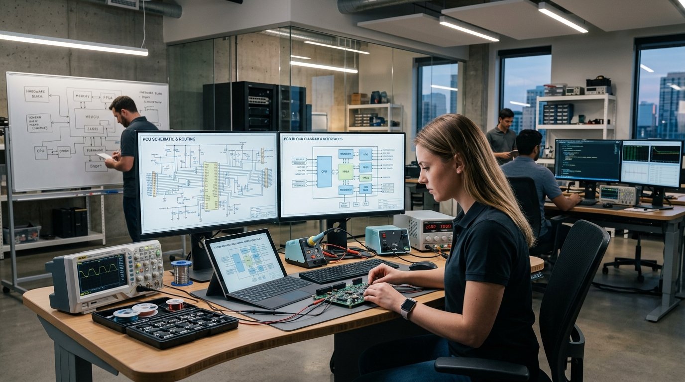
Every successful industrial project starts with crisp scoping. We translate business intent into technical Product Requirement Documents (PRDs), perform target cost BOM modeling, and establish regulatory roadmaps before laying down a single trace.
Our 50+ multidisciplinary engineers execute schematic capture, high-speed PCB layouts (up to 32 layers), micro-via fanouts, firmware architecture, and mechanical enclosure engineering with comprehensive thermal simulation.
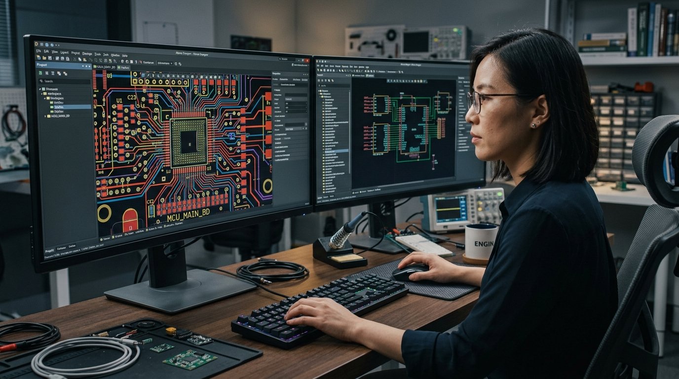
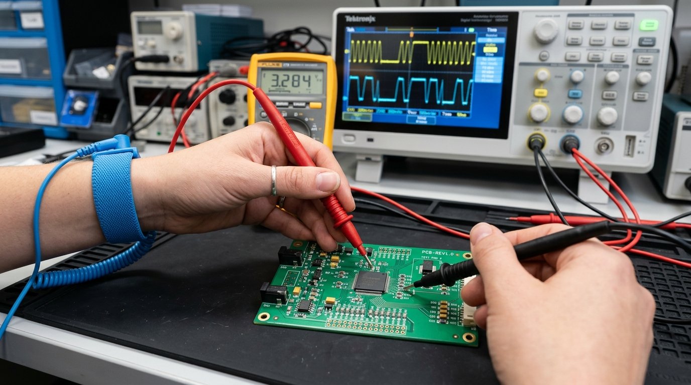
Fast-turn prototypes (24 to 48 hour turnaround on PCBA) allow physical testing before committing to production tooling. We subject builds to stringent DFM (Design for Manufacturing) and DFA (Design for Assembly) reviews.
Direct relationships with global semiconductor manufacturers and tier-1 franchised distributors guarantee authentic components, optimum pricing, buffer stock agreements, and domestic value addition (DVA).
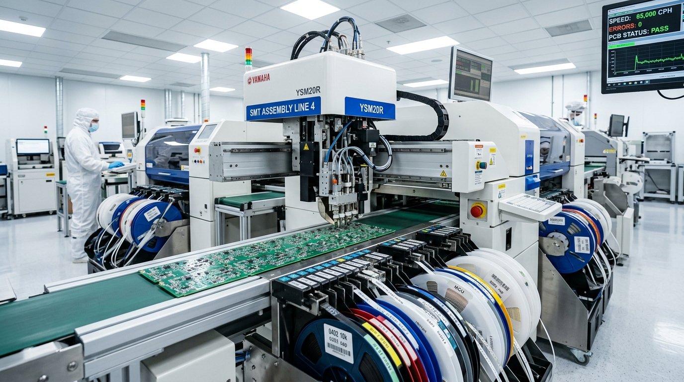
Equipped with high-speed Fuji & Yamaha lines in ISO 8 / Class 100,000 cleanrooms, 10-zone Nitrogen reflow ovens, automated Komax wire harness crimpers, 80T–1,700T injection moulding, and robotic CNC sheet metal fabrication.
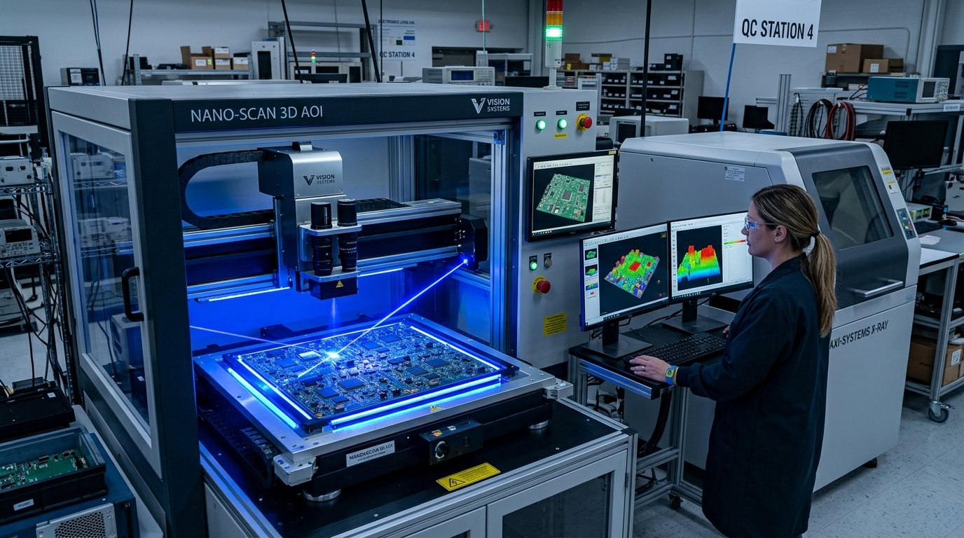
Zero-defect policy backed by 100% in-line 3D AOI, 2D/3D X-Ray inspection of BGA solder joints, In-Circuit Testing (ICT), custom bed-of-nails functional test benches (FCT), and environmental burn-in stress screening.
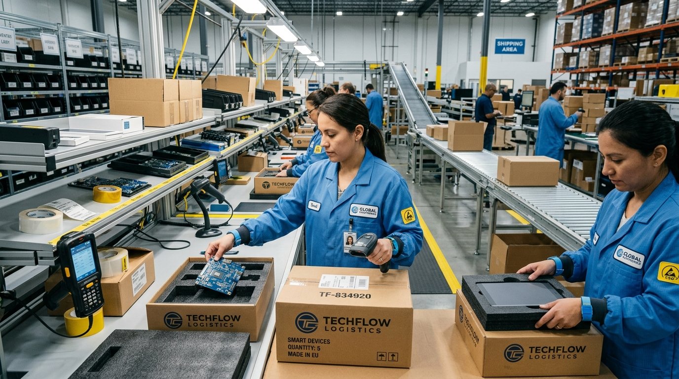
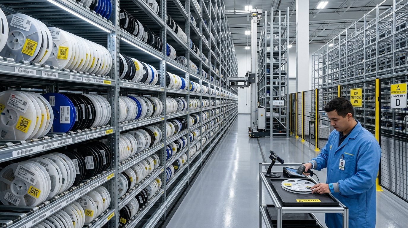
When you scale, our supply chain and logistics engine ensures flawless delivery. Every box and board is serialized with laser QR codes, maintained in climate-controlled ESD warehousing, and shipped via Kanban JIT line feeding.
| Category | Engineering Limit / Capability | Equipment / Technology |
|---|---|---|
| PCB Fabrication | 1 to 32 Layers, Rigid, Flex, Rigid-Flex; Min Trace/Space 2.5 mil / 2.5 mil; Blind & Buried Vias, Microvias | Laser Direct Imaging (LDI), Vertical Continuous Plating, Automated Optical Inspection |
| SMT Placement | Component sizes from 01005 passives up to 100mm² ICs; BGA/Micro-BGA pitch down to 0.3mm; PoP (Package-on-Package) | Fuji & Yamaha High-Speed Pick & Place, 10-Zone Nitrogen Reflow, Koh Young 3D SPI |
| Inspection & Test | 100% 3D AOI inspection; 2D/3D X-Ray (void ratio < 10%); In-Circuit Testing (ICT); Flying Probe; Boundary Scan (JTAG) | TRI 3D AOI, Nordson Dage X-Ray, Keysight ICT, Takaya Flying Probe, Thermal Chambers |
| Wire Harness | 10 AWG to 32 AWG; High-Voltage EV orange cables; Multi-core shielded harnesses; Ultrasonic wire splicing | Komax Alpha 355/550, Schleuniger Strip Series, Cirris Computerized Continuity Testers |
| Plastic Moulding | Tonnage 80T to 1,700T; Part weight from 2g to 12kg; Precision hot-runner tooling; Optical and engineering grades | Engel, Toshiba, Haitian servo-hydraulic moulding machines, Sepro robotic parts extractors |
| Sheet Metal | Thickness 0.5mm to 16mm (CRCA, Stainless, Aluminum); ±0.05mm cutting tolerance; Robotic MIG/TIG/Spot welding | 4kW/6kW Fiber Laser Cutters, CNC Synchronized Press Brakes, 7-Tank Pretreatment Powder Line |
This seven-stage journey is the core operating proposition connecting your product intent to dependable volume production.